- 23 5 月 2024
- By: jimmy@otomosemi.com
PCB Manufacturing and Assembly
Printed circuit
Read MoreHXPCB focuses on the research and development of ultra-large size circuits board, multi-layer PCBs, metal-based PCBs, rigid-flex high-frequency PCBs, HDI PCBs, and related processes. We offer comprehensive services, including PCB design, prototyping, processing, and assembly.




.jpg)
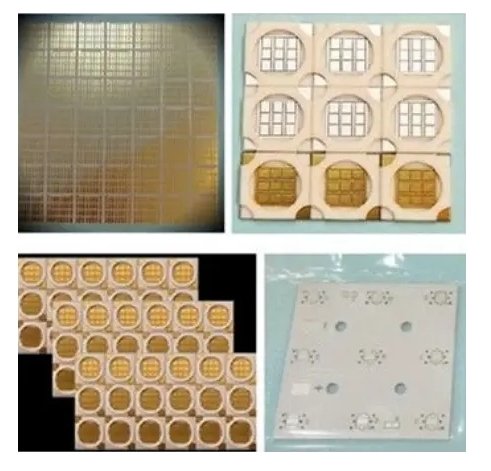
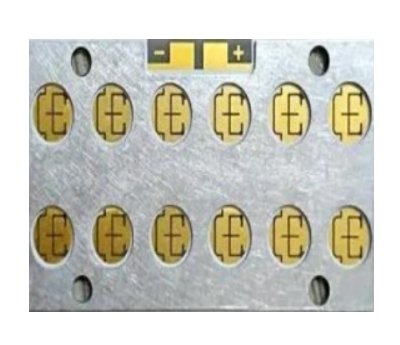
Ceramic PCB is a printed circuit board that uses ceramic material as the substrate. Compared with traditional FR4 or metal substrate PCB, ceramic PCB has excellent thermal conductivity, mechanical strength and high temperature stability, and is widely evaluated in electronic products that require higher performance, especially in high power, high frequency and high temperature environments.
The thermal conductivity of ceramic materials is usually times higher than that of metal and traditional FR4 materials, and they can work more efficiently.
Ceramic PCBs have lower dielectric constants and lower electrical losses, and perform extremely well in high-frequency and RF applications.
Ceramic PCBs can operate at higher operating temperatures, usually able to withstand temperatures above 300°C, while the upper temperature limit of ordinary FR4 materials is about 130°C.
Ceramic materials themselves have high mechanical strength and impact resistance, and can withstand greater physical stress.
Ceramic PCBs have very good dimensional stability when the temperature changes, especially suitable for applications that require precise dimensional control.
Single-Sided Ceramic PCB is a circuit laid out on one side of a ceramic substrate. It is usually used in simple circuit designs, and is common in low-power LED lighting, sensors and other applications.
Double-Sided Ceramic PCB is a circuit laid out on both sides of a ceramic substrate, and is suitable for more complex circuit designs. It can improve the integration of components and save space.
Multilayer Ceramic PCB is composed of multiple layers of ceramic substrates, and each layer is connected by a highly conductive metal layer. This design is suitable for high-density, high-frequency and high-power applications.
Substrate preparation
The substrate of ceramic PCB usually adopts ceramic materials such as aluminum oxide (Al2O3), aluminum nitride (AlN), silicon nitride (SiN). The preliminary process includes cutting the ceramic material into the required size and shape.
Circuit pattern transfer
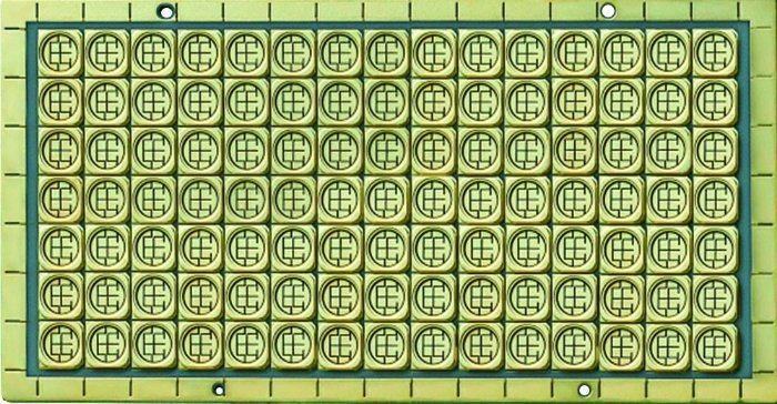
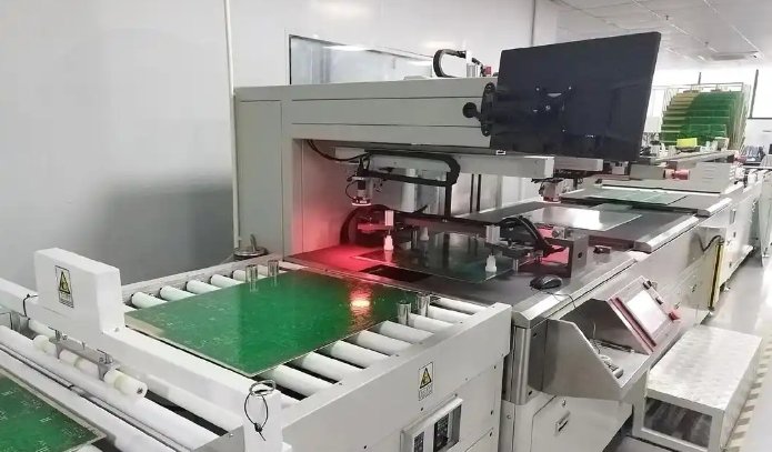
A layer of photoresist is applied to the surface of the ceramic substrate, and then the circuit pattern is transferred to the photoresist by ultraviolet light irradiation. Then it is developed to leave the graphics of the circuit pattern, and then according to the design requirements, holes are punched on the ceramic substrate to form the necessary electrical connection channels.
Electrode deposition
Conductive metals (such as gold, silver, copper, etc.) are deposited on the surface of the ceramic substrate through evaporation, sputtering or chemical vapor deposition (CVD) and then the metal layer is thickened by electroplating to ensure the conductivity of the circuit.
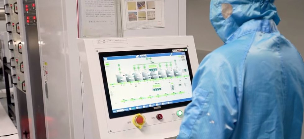
Sintering process
After the metal deposition is completed on the ceramic substrate, sintering treatment is required to ensure good bonding between the metal and the ceramic substrate.
Surface treatment
After the circuit pattern and metal deposition are completed, the ceramic PCB is surface treated, such as tin plating, gold plating, etc., to improve weldability and reliability.
The equipment costs of ceramic materials and special processes (such as laser processing, DPC, LTCC) are high, resulting in a significant increase in overall manufacturing costs compared with traditional PCBs.
Precision pattern transfer
Ceramic substrates require high-precision circuit patterns, and the ceramic surface is hard and irregular, which increases the complexity of processes such as photolithography and laser marking.
Ceramic materials (such as aluminum oxide, aluminum nitride, silicon nitride) have high hardness and brittleness, and are prone to cracks and fragments during processing, making manufacturing more difficult.
The bonding strength between the ceramic substrate and the metal layer (such as copper, silver) is difficult to ensure, especially in high temperature or high humidity environments, which is prone to delamination or peeling.
Although ceramic materials have low dielectric loss, material purity and surface quality still need to be strictly controlled in high-frequency applications to reduce signal loss and reflection.
Ceramic materials have high hardness, and micro-hole processing (such as through holes or blind holes) can easily cause chipping or processing deviations.
LED lighting
LED street lights, car headlights, projector light sources
Engine modules
5G communication equipment, 5G base stations and RF modules, filters, amplifiers, antenna arrays and other RF components.
Microwave and millimeter wave applications
Radar systems, satellite communication equipment, high-frequency radio frequency identification (RFID), etc.
In-vehicle radar
Advanced driver assistance systems (ADAS) such as cruise control, blind spot detection, and traction maintenance.
Power system
Automotive power control unit (PCU), battery management system (BMS)
Implantable medical devices
Pacemakers, stair-type hearing devices, etc.
High-precision medical instruments
CT scanners, ultrasound equipment and laboratory analysis instruments.
Industrial control
High-voltage relays, control modules.
Military industry and defense
Military radar and communication equipment, missile control systems
New energy equipment
In solar photovoltaic devices, wind power control power generation systems
| Parameter | Typical Value/Range | Description |
| Base Material | Al₂O₃ (Alumina) | Common material used in ceramic substrates. |
| Thermal Conductivity | Aluminum (Al) | Indicates the material’s ability to conduct heat. |
| Dielectric Constant (Dk) | Al₂O₃: 9.8, AlN: 8.6, Si₃N₄: 7.8 | Measures the material’s ability to store electrical energy. |
| Dielectric Loss (Df) | Al₂O₃: 0.001, AlN: 0.0005 | Determines the energy lost in signal transmission. |
| Coefficient of Thermal Expansion (CTE) | Al₂O₃: ~7 ppm/°C, AlN: ~4 ppm/°C, Si₃N₄: ~3 ppm/°C | Shows how the material expands with temperature. |
| Substrate Thickness | 0.25 mm – 1.5 mm | Available thickness of ceramic substrates. |
| Metal Layer Thickness | 10 µm – 500 µm | Thickness of conductive metal (e.g., copper, silver). |
| Working Temperature | -55°C to 850°C | The operational temperature range. |
| Breakdown Voltage | >15 kV/mm | Indicates insulation strength under high voltage. |
| Surface Finish | ENIG, Silver, Gold | Surface coatings to enhance solderability and protect the metal. |
| Metal Adhesion Strength | >10 N/mm | Bonding strength of the metal layer to the ceramic. |
HXPCB provides high-performance ceramic PCB integration services that can meet the needs of high-power, high-frequency and high-reliability applications. These include ceramic circuit board solutions in multiple fields such as LED lighting, 5G communications, automotive radar, medical equipment, etc. HXPCB focuses on precision manufacturing and reliable assembly processes to ensure the excellent performance and stability of ceramic PCBs in various environmental extremes.
Yes, ceramic PCBs can operate at temperatures as high as 850°C due to the inherent heat resistance of ceramic materials like AlN and Si₃N₄.
Ceramic PCB substrates are available in thicknesses ranging from 0.25 mm to 1.5 mm, while the metal layer (e.g., copper or silver) can range from 10 µm to 500 µm, depending on the application requirements.
Ceramic PCBs have high thermal conductivity, enabling efficient heat dissipation, which is crucial in high-power applications. Their low thermal expansion and excellent electrical insulation ensure stability and reliability under extreme conditions.
Ceramic PCBs typically use aluminum oxide (Al₂O₃), aluminum nitride (AlN), and silicon nitride (Si₃N₄) as the substrate materials. Each material offers unique thermal and dielectric properties:
Al₂O₃: Affordable and widely used, with moderate thermal conductivity.
AlN: High thermal conductivity and good electrical insulation.
Si₃N₄: Excellent mechanical strength and thermal stability.
Surface finishes include ENIG (Electroless Nickel Immersion Gold), silver plating, and gold plating. These finishes enhance solderability and protect the metal layer from oxidation.
LED lighting: High-power LEDs, automotive lighting.
5G and RF communications: Filters, amplifiers, antennas.
Automotive electronics: ADAS, radar systems, power control units.
Medical devices: Implantable devices, high-precision diagnostic equipment.
Aerospace: Satellites, avionics.
Yes, ceramic PCBs are ideal for high-frequency applications due to their low dielectric constant (Dk) and dielectric loss (Df), ensuring minimal signal distortion and loss.
Thermal Conductivity: Ceramic PCBs far outperform FR4 in heat dissipation.
Operating Temperature: Ceramics can handle much higher temperatures.
Electrical Performance: Ceramic PCBs have lower dielectric losses, making them ideal for high-frequency applications.
However, ceramic PCBs are generally more expensive and harder to process.
There are many v
Read More